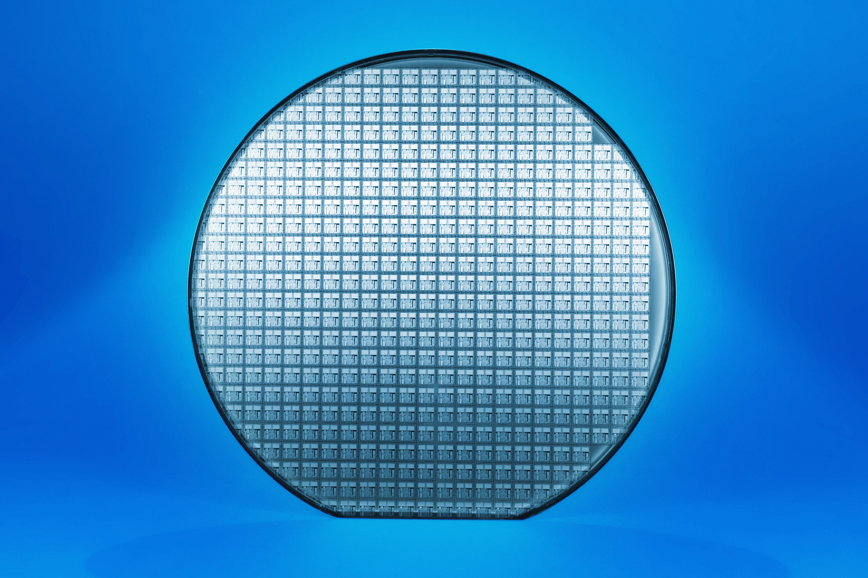
TSMC laid out a dazzling array of technologies at its 2025 Europe Technology Symposium in Amsterdam yesterday.
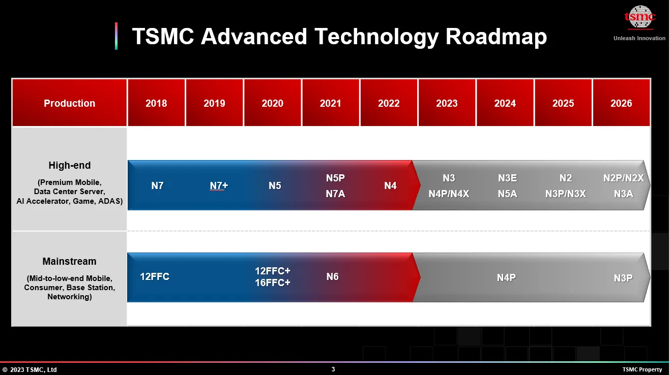
Starting with the ‘last and best finfet node’’ – N3 – TSMC said it expects the process to be a high-volume and long-running node with more than 70 new tape-outs as of April 2025.
N3E is already in high-volume production of flagship mobile and HPC/AI products.
N3P entered volume production in Q4 2024.
Additional N3 variants include:
N3X pushes the performance envelope for client CPUs.
N3C enhances cost effectiveness for value-tier products.
N3A targets automotive applications, including driver assistance and self-driving technology. Currently undergoing final defect improvements and on track for AEC-Q100 Grade 1 qualification.N3A will be production-ready later in 2025.
Following N3 comes N2 which is on track for production in the second half of 2025.
256Mb SRAM average yield is over 90%.
The number of N2 second-year new tape-outs has grown 4X versus N5 in the same period.
N2P is on track for production in the second half of 2026.
Compared with the N3E process, N2P will offer:Up to 18% speed improvement at the same power
Approximately 36% power reduction at the same speed
1.2X logic density
N2X will offer approximately 10% Fmax (maximum clockof technologies at itsc frequency) and is scheduled for production in 2027
After N2 will come A16 which offers best-in-class backside power delivery and improved logic density for datacentre AI/HPC products that have demanding signal routing and power delivery requirements.The development of A16 is on track and will be ready for production in 2H26.
A16’s successor, A14, will accelerate AI momentum and supercharge on-board smartphone AI capabilities with more powerful computing and greater power efficiency.
Compared with the N2 process, A14 will offer:
Up to 15% speed improvement at the same power
Up to 30% power reduction at the same speed
More than 20% increase in logic density
A14 will incorporate new NanoFlex Pro technology to enable greater performance, power efficiency, and design flexibility.
A14 is scheduled to enter production in 2028, and a Super Power Rail version is planned for 2029.
Then comes the vista beyond N2 with a promising scaling candidate in the complementary field-effect transistor (CFET) design which caters to the increasing demand for improved performance and reduced power consumption in a compact form factor
By stacking the nFET and pFET vertically, CFET achieves nearly twice the
density.
At IDEM this year, TSMC integrated nFET and pFET on the same wafer and
presented the world’s smallest CFET inverter at 48nm gate pitch.
TSMC has also made progress on transistors with 2D materials, the thinnest channel in the company’s research portfolio.
TSMC demonstrated a first electrical performance using a monolayer channel in a stacked nanosheet transistor architecture similar to the N2 technology node.
3D Fabric Technologies: The SoIC platform is for 3D silicon stacking and consists of SoIC-P and SoIC-X, two stacking schemes.
SoIC technology for N3-on-N4 stacking will enter production in 2025, with 6µmpitch. Next-generation SoIC A14-on-N2 will be ready in 2029.
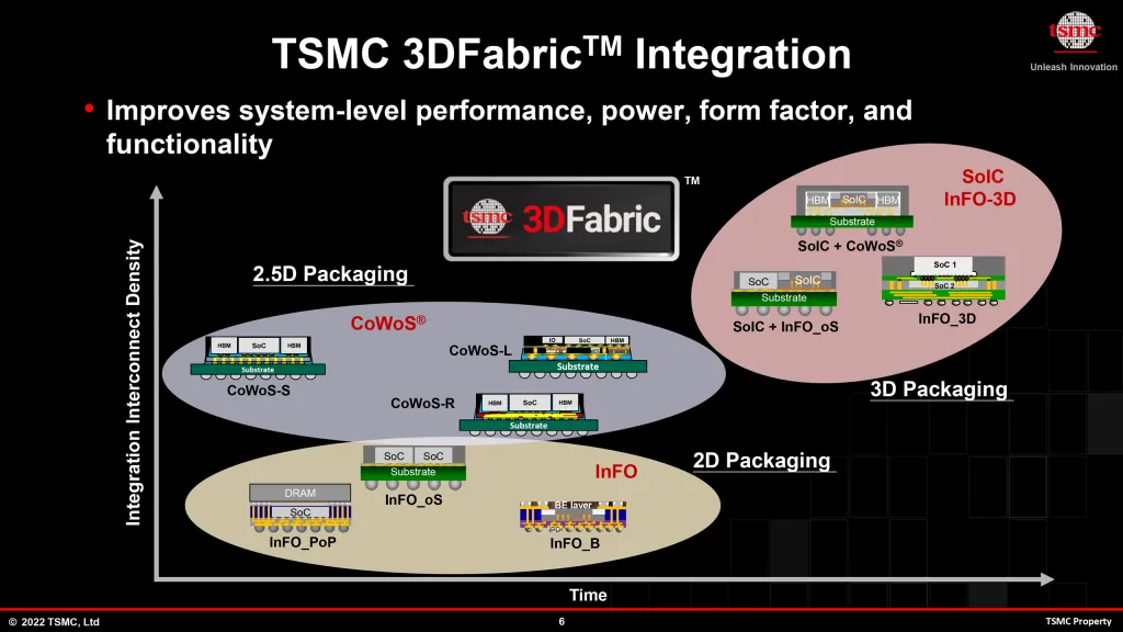
InFO PoP and InFO-3D are aimed at high-end mobile applications and InFO 2.5D at chiplet integration for HPC.
A key enabler of AI training and inference, Si interposer-based CoWoS-S and RDL interposer-based CoWoS-L and R aim to integrate advanced logic and HBM for HPC applications.
A larger reticle size enables more chips to be integrated into the same package. This allows for more efficient integration of multiple smaller chips (chiplets) and memory stacks (like HBM) onto a single, larger interposer. The 5.5-reticle CoWoS-L will be offered in 2026.
TSMC is pushing the boundaries with a 9.5 reticle size CoWoS. Volume production is scheduled for 2027.
This size offers the integration of 12 or more HBM stacks in a package, together with TSMC’s leading-edge logic technology, to support bigger AI accelerator designs.
System-on-Wafer (TSMC-SoW) Technology:
An innovative wafer-scale integration of logic and HBM to meet surging demand invcomputing power for AI training
The SoW platform integrates all necessary components together, such as the connector, power module, and cooling module.
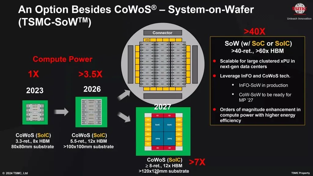
TSMC introduced SoW-X, a CoWoS-based offering and wafer-sized system with
computing power 40X greater than the current CoWoS solution, on par with an entire server rack. SoW-X is scheduled for volume production in 2027.
Specialty Technology: To advance the AI future, TSMC offers:
An industry-first HBM base-die using advanced logic for HBM4 migration, enabling high performance and lower power consumption.
The N12 base-die solution (offering more than 40% power reduction) is ready, and the N3 base-die solution will be ready by the end of 2025.
Co-packaged silicon photonics for bandwidth scaling. Optical transceivers enable high-speed, low-energy, reliable data transmission.
TSMC’s SoIC technology stacks electrical and photonic die for higher interconnect density and lower system power. Going from board-level to interposer-level optical engine integration offers more than 10X the power benefit.
A new Integrated Voltage Regulator (IVR) for AI with 5X vertical power density delivery compared with a separate power management chip on the circuit board.
As AI GPU power is reaching kilowatt levels, this functionality becomes even more necessary.
High-density embedded deep trench capacitor (eDTC) and deep trench capacitor (DTC) provide good power stabilization for switching regulators and logic die.
Smart vehicle technology includes:
Automotive-grade advanced packaging
Lateral overflow integration capacitor (LOFIC) image sensors for high dynamic range to handle sudden changes in light conditions, enabled by TSMC’s 3D high-density metal-insulator-metal (MiM) capacitor
For automotive ADAS, it provides a more than 100 dB LED flicker-free
dynamic range without compromising light performance and generation.
16FFC RF process for millimeter-wave radar
Next-generation resistive random-access memory (RRAM) and magnetoresistiverandom-access memory (MRAM). 28nm RRAM is qualified for automotive applications, and 12nm RRAM is expected to meet the same stringent automotive low PPM requirements.
22nm MRAM is in production, and 16nm MRAM is ready for customers. 12nm MRAM is in development.
TSMC is validating MRAM and RRAM for future scalability down to 5nm and 6nm respectively.
TSMC supports IoT applications with the following technology:
Begun exploratory development of N4e, aiming for continued Vdd (positive power supply voltage) reduction.
Additionally, ultra-low leakage SRAM and logic further reduce leakage power to extend battery life.
TSMC’s advanced RF technologies provide effective power and area scaling to boost product competitiveness and optimise user experience. These technologies have enhanced features such as analogue cells, LDMOS, low Vdd coverage, and low noise devices.
As AI begins to move to the edge in smartphones and beyond, TSMC launches N4C RF, the next generation of TSMC’s radio frequency technology from N6RF:
Delivers 30% power and area reduction versus N6RF+.
Designed to provide high-speed, low-latency wireless connectivity to transfer large amounts of data, N4C RF will meet emerging standards such as Wi-Fi 8 and AI-rich True Wireless Stereo.
Scheduled to enter risk production in Q1 2026.
In display technologies, TSMC announced the industry’s first FinFET high voltageplatform to be used in foldable/slim OLED and AR glasses. Compared to 28HV, 16HV is expected to reduce DDIC power by around 28% and increase logic density by approximately 41%.